


Vision Chip developed by Sony and Ishikawa Watanabe Laboratory of the University of Tokyo
Summary
Sony and Ishikawa Watanabe Laboratory of the University of Tokyo developed a Vision Chip for high-speed and robust visual feedback systems. The developed Vision Chip secures large areas of PE and PD by stacking peripheral circuits including PEs and memory with imager and realizes both of high imaging capability and high functionality. PD part is fabricated by 90nm process and forms 1/3.2-inch, 1.27Mpixels, back-illuminated sensor. PE part is fabricated by 40nm process and mounts column-parallel PEs, column-parallel ADCs and frame memory for 1ms high-speed image processing. The programmable PE can implement high-speed spatio-temporal filtering and enables imaging and various image processing such as detection, recognition and tracking on one chip. By realizing image processing on the chip, the vision chip can suppress power consumption to max 363mW @1000fps and will keep or improve the performance and save space and energy comparison with conventional system which has sensors and processors separately.
At the conference of solid-state circuits, ISSCC 2017 held in Feb. 2017, Sony and Ishikawa Watanabe Laboratory of the University of Tokyo demonstrated 1ms target recognition and tracking by programming spatio-temporal image processing on the 140GOPS column-parallel SIMD PEs. As the demonstration, Vision Chip is expected to provide high-speed, low-latency, low-power and small-sized visual feedback systems.
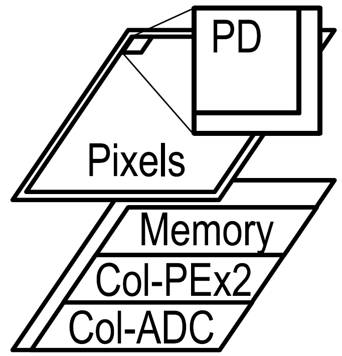
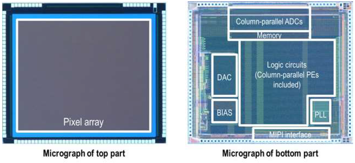
Fig. 1: Vision Chip Architecture and Micrograph*1.
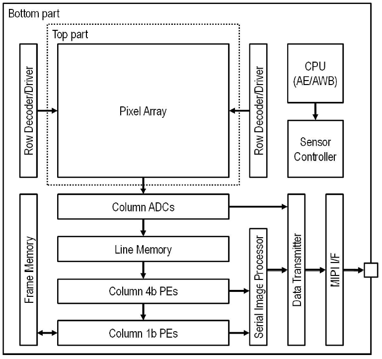
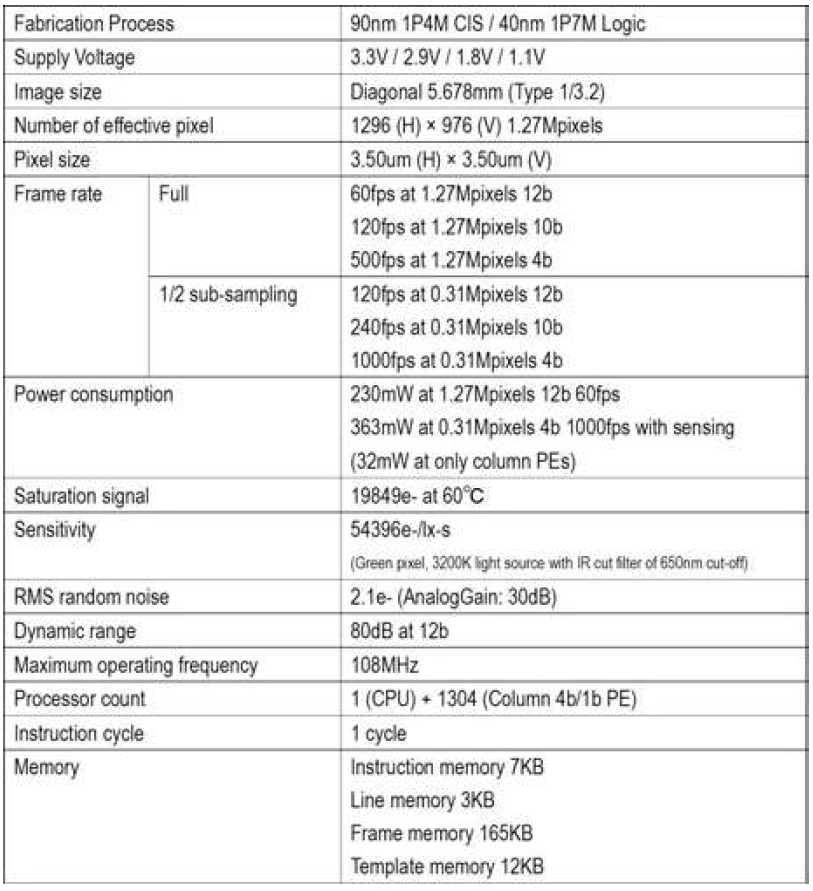
Fig. 2: Block Diagram and Specifications*1.
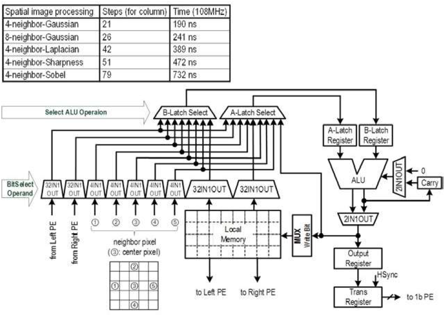
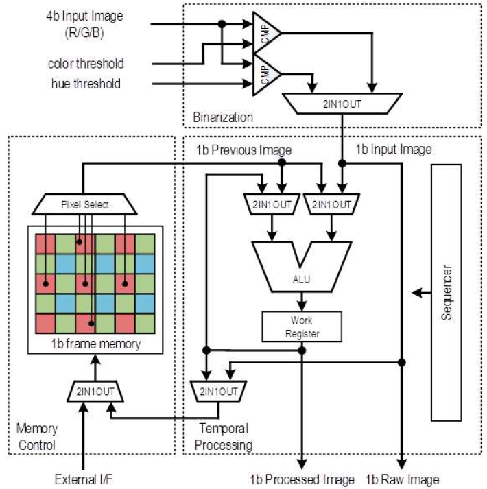
Fig. 3: Schematic of the PE*1.
*1 Image credit : T. Yamazaki, H. Katayama, S. Uehara, A. Nose, M. Kobayashi, S. Shida, M. Odahara, K. Takamiya, Y. Hisamatsu, S. Matsumoto, L. Miyashita, Y. Watanabe, T. Izawa, Y. Muramatsu, M. Ishikawa : A 1ms High-Speed Vision Chip with 3D-Stacked 140GOPS Column-Parallel PEs for Spatio-Temporal Image Processing, International Solid-State Circuits Conference (ISSCC 2017), Proceedings, pp.82-83, San Francisco, California, USA, 5-9 Feb. (2017)
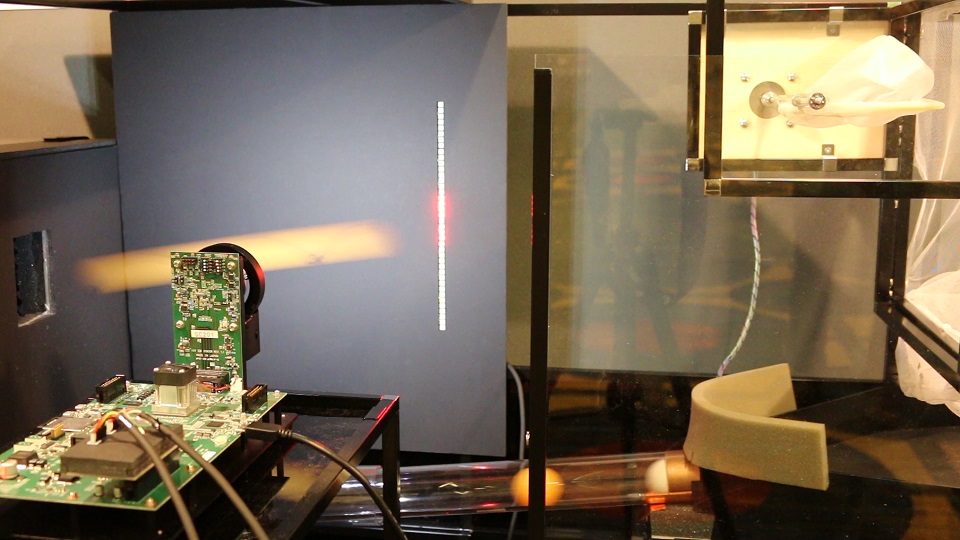
Fig. 4: Vision Chip Demo System at ISSCC 2017
Movie
If you want to use the original video, please send an e-mail for copyright permission to contact .
References
- T. Yamazaki, H. Katayama, S. Uehara, A. Nose, M. Kobayashi, S. Shida, M. Odahara, K. Takamiya, Y. Hisamatsu, S. Matsumoto, L. Miyashita, Y. Watanabe, T. Izawa, Y. Muramatsu, M. Ishikawa : A 1ms High-Speed Vision Chip with 3D-Stacked 140GOPS Column-Parallel PEs for Spatio-Temporal Image Processing, International Solid-State Circuits Conference (ISSCC 2017), Proceedings, pp.82-83, San Francisco, California, USA, 5-9 Feb. (2017)