|
|
A Software-Controlled Pixel-Level A-D Conversion Method |
[English | Japanese]
A pixel-level analog-to-digital (A-D) conversion method suitable for digital vision chips is proposed. In this method, each quantization boundary is compared by determining whether the signal level integrated for a certain time has reached a certain voltage, where both the time and voltage are properly controlled by software for each boundary. We derive an algorithm to generate an optimal controlling schedule to realize an arbitrary A-D conversion scale subject to the condition that noise is minimized. Experimental results show that images with given A-D characteristics can be obtained with low noise.
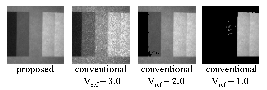
Fig. 1: Images of a grayscale chart obtained with linear
characteristics. The proposed method can overcome the tradeoff that
existing methods have between image noise and lower detection limits.
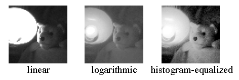
Fig. 2: Images obtained with different characteristics. The results
show that the proposed method can achieve wide dynamic range imaging
by realizing adequate A-D conversion scales.
*IEEE © 2003 IEEE. Personal use of this material is permitted. However, permission to reprint/republish this material for advertising or promotional purposes or for creating new collective works for resale or redistribution to servers or lists, or to reuse any copyrighted component of this work in other works must be obtained from the IEEE.
[ Home | Sensor Fusion | Visual Servo | Vision Chip | Optics in Computing | Members | Papers ]
Ishikawa Nami Komuro laboratory WWW admin: www-admin@k2.t.u-tokyo.ac.jp